
Similar processing technology for thin-film solar cells
The main processing steps of thin-film solar cells include: battery core board, sandblasting or laser treatment around the battery, ultrasonic welding, inspection, lamination, frame mounting, junction box mounting, wire clamp connection, packaging, etc.
There are three main manufacturing processes for thin-film solar cells. The first is a single-chamber, multi-piece glass substrate manufacturing technology. This technology is mainly represented by Chronar, APS, and EPV in the United States; the second is a multi-chamber, two-piece (or Multi-piece) glass substrate manufacturing technology, this technology is mainly represented by Japan KANEKA company; the third type of winding flexible substrate manufacturing technology, the substrate is mainly stainless steel, polyimide, this technology is mainly based on the United States Uni-Solar company to represent.
There are many domestic equipment manufacturers in China. Each production line uses only one vacuum chamber for amorphous silicon deposition. The vacuum chamber can be equipped with 2 deposition fixtures, or 3 deposition fixtures, or 4 deposition fixtures; there are also amorphous silicon for each production line There are 2 empty chambers or 3 vacuum chambers for silicon deposition, and each vacuum chamber can be equipped with 2 deposition fixtures or three deposition fixtures. In short, the main domestic amorphous silicon battery production lines, whether imported or domestic, mainly use single-chamber, multi-piece glass substrate manufacturing technology.
The back electrode of the battery usually adopts the method of aluminum plating. There are two methods of aluminum plating. One is evaporation aluminum plating. The process is simple, the equipment is small, the equipment investment is low, and the operating cost is relatively low, but the film thickness is uneven and the mask effect is difficult. It is guaranteed that the operation is labor-intensive and is suitable for coating small areas. The second type is magnetron sputtering aluminum plating. The film has good uniformity, firmness, and quality assurance. It is suitable for large-area aluminum plating. The disadvantage is that the equipment investment is large and the operating cost is high.
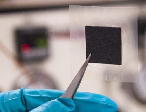
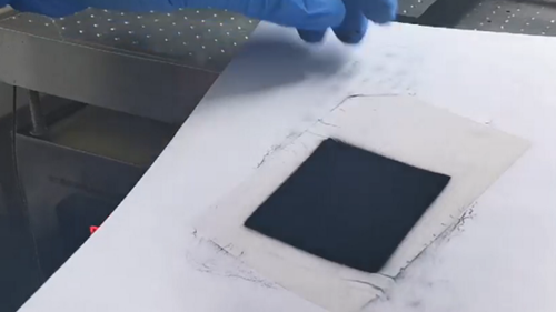
A low-cost, non-vacuum mechanochemical method and spin-coating/selenization method are used to prepare the chalcopyrite structure CIGS thin film light absorption layer for solar cells. The non-vacuum mechanical ball milling method prepared the chalcopyrite-type CIGS nano-powder material, the structure and morphology of the CIGS nano-powder were prepared systematically, using a practical and efficient rapid heating heat treatment furnace, and the non-vacuum spin coating method was used to prepare the flash Zinc ore structure CZTSe precursor film.
The RF magnetron construction method is used to prepare a flat, dense and columnar MO bottom electrode layer film. As the sputtering power increases, the working pressure increases, the target base distance decreases, and the film crystallinity becomes more complete.
The chemical water bath deposition method prepares CdS thin films with a flat surface and a tetragonal structure. With the extension of the water bath reaction time, the intensity of the main diffraction peaks of the CdS film on the test surface of the XRD structure gradually increases, which can effectively reduce the voids of the CdS film, and the light transmittance exceeds 70%. As the deposition time of the chemical bath increases, the light is transmitted The rate gradually decreases.
Perovskite Spraying Video
https://www.youtube.com/watch?v=I4aIprqeekk
Recommended Machine
UAL100 ultrasonic dispersion liquid supply system
UAM3000 Ultrasonic Bracket Spraying Machine
UAM4000 small desktop ultrasonic spraying machine
UAM4000L Ultrasonic Precision Spraying Machine
UAM6000 Ultrasonic Large Spraying Machine
UAM7000 Ultrasonic Balloon Guide Wire Spraying Machine
UAM8000 ultrasonic assembly line spraying machine

