Photoresist Coating
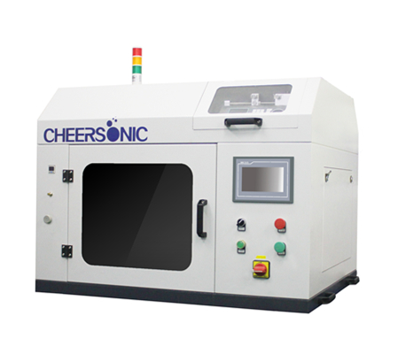
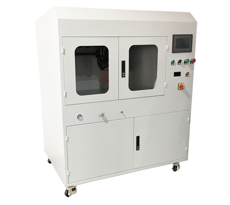
Ultrasonic spraying technology is used for semiconductor photoresist coating. Compared with traditional coating processes such as spin coating and dip coating, it has the advantages of high uniformity, good encapsulation of microstructures, and controllable coating area. In the past 10 years, it has been fully demonstrated that the 3D microstructure surface photoresist coating using ultrasonic spraying technology, the prepared photoresist coating is significantly higher than the traditional spin coating in terms of microstructure wrapping and uniformity Craft.
The ultrasonic spraying system can precisely control the flow rate, coating speed and deposition volume. Low-speed spray shaping defines atomized spray as a precise and controllable pattern to avoid excessive spray when producing a very thin and uniform layer. The ultrasonic spray system can control the thickness from sub-micron to more than 100 microns, and can coat any shape or size.
Application
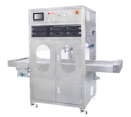
Ultrasonic spraying system can be used for surface coating of flat and 3D structural substrates including silicon wafers, glass, ceramics, metals and other materials. Typical photoresist coating applications include wafers, MEMs, lenses, microfluidic chips, filters and many more.
Advantages of ultrasonic spraying for photoresist:
• High uniformity and uniformity
• Non-contact spraying
• Micro-flow spraying, multiple liquid feeding schemes
• High speed control accuracy
• High liquid utilization
• High flexibility in chemical and coating performance.
• Non-clogging atomized spray.
• High transmission efficiency and minimal waste.
• Highly repeatable mature spraying process.
Photoresist Spray Video
https://www.youtube.com/watch?v=nvkEyfP90Qk